
This article is adapted from a Statementdog podcast featuring interviews with Chu Ming-kuei, Chairman of PVI, and Yang Wei-wen, General Manager of IV Technologies.
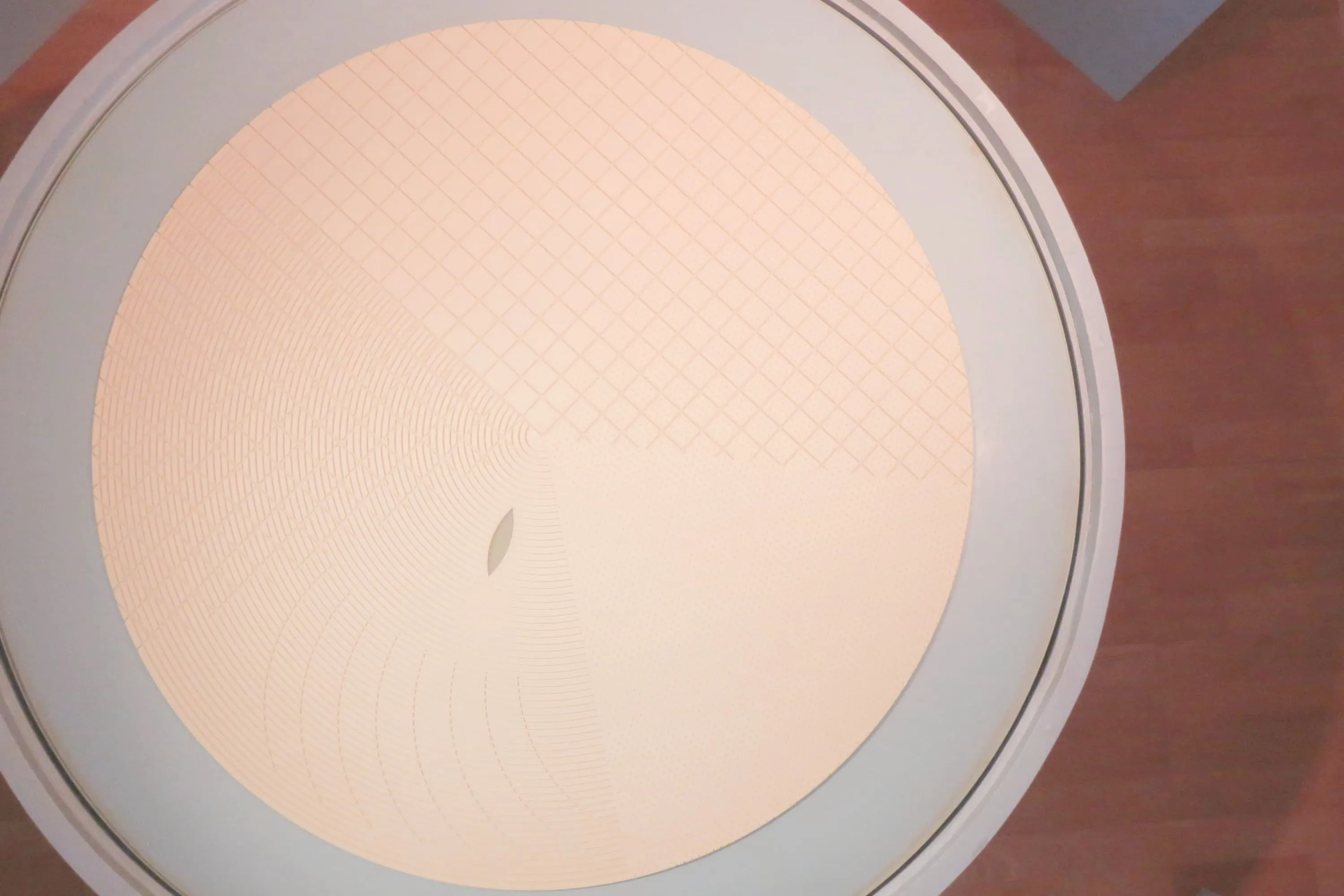
A polishing pad shown on IV Technologies’ official website. Its concentric and crosshatched grooves illustrate how pad design shapes slurry distribution. Image: IV Technologies.
As semiconductor manufacturing advances toward smaller nodes, processes become more complex, driving up the consumption of consumables. For example, Chemical Mechanical Polishing (CMP) now requires more steps due to process scaling. Furthermore, advanced packaging has introduced CMP processes not found in traditional packaging. These trends have created a massive opportunity for semiconductor consumable suppliers. PVI (頌勝科技) and its subsidiary, IV Technologies (智勝科技), are Taiwanese suppliers pursuing this market. The interview describes their development and qualification experience; it does not establish an exhaustive count of domestic suppliers.
IV Technologies’ official product information describes several pad families and customized groove designs. This supports the discussion of its product range and customization, while the company history and litigation account below remain attributed to the podcast interview.
From a PU Formulator to a Semiconductor Supplier
Founded in 1986, PVI began as a polyurethane (PU) chemical formulator. The 1997 Asian Financial Crisis spurred the company to pivot toward high-value-added products. After exploring shoe materials and automotive parts, PVI found success in the medical materials sector, forging a partnership with a top US brand for therapeutic footwear that the interview describes as a long-running customer relationship.
In 2000, an acquaintance presented a polishing pad, noting it was produced by only one American company and commanded a very high price. PVI analyzed it and confirmed it was a PU product — something they were capable of manufacturing. The team spent two years studying the patent landscape, aiming not just to avoid infringement but to engineer around existing patents to create a functional, viable alternative.
After successful in-house trials, PVI assembled a team of over a dozen experts in PU materials, semiconductor equipment, process applications, and machining, spinning them off to form IV Technologies.
The General Manager of IV Technologies brought a deep semiconductor background, having started his career in process integration at a systems fab. After that company was acquired by UMC, he pivoted to Taiwan’s nascent OLED panel industry before joining IV Technologies, where he has now been for 20 years.
The Unique PU Technology for Polishing Pads
While made of PU, these pads are fundamentally different from the PU familiar to consumers in running tracks, mattresses, or mouse pads. PU is a polymer, and different formulations create entirely different products.
PVI’s confidence in entering this market stemmed from its dual mastery of two key technologies: “micro-porous foaming” and “elastomers.” The pad itself is a “micro-porous” PU foam, but it requires an “elastomer” window for detecting the polishing endpoint. Most Taiwanese PU plants specialize in one area, like foam for sofas or materials for running tracks. Few manufacturers, like PVI, were proficient in both complex technologies: high-performance elastomers (like those in roller-skate wheels) and foamed materials.
Even with PU expertise, breaking into semiconductors was a different world. IVT’s success hinged not only on PVI’s deep formulation knowledge but also on leadership’s trust in its professional team. The difficulty in the semiconductor industry is not making “one functional pad,” but ensuring “consistent, long-term, stable production” of that pad.
CMP Complexity and IVT’s Customization Advantage
CMP is one of the most complex processes in chipmaking. The pad’s stability is crucial, but it must also work in harmony with the slurry, the diamond disk (pad conditioner), and the client’s preceding and subsequent process materials. To succeed, a supplier must deeply understand CMP technology, application integration, and pass rigorous client qualifications while maintaining long-term quality. IVT spent its first two years on patent research and adopted a production technology entirely different from its competitor.
CMP (Chemical Mechanical Polish) is essential for planarization. Semiconductor manufacturing involves stacking multiple dielectric and conductive layers. After each layer is deposited, it must undergo photolithography. The focus accuracy of this exposure process is critically dependent on the “flatness” of the wafer surface — this is CMP’s primary job. As nodes advance, the precision required for exposure increases, making CMP ever more critical.
-
The “Chemical” aspect is handled by the slurry, which reacts with specific materials (like copper or tungsten) to make them easier to remove.
-
The “Mechanical” aspect is performed by the polishing pad. The slurry must be distributed across the pad. The pad’s porous PU material and its surface groove design ensure proper slurry distribution, which, combined with mechanical rotation, performs the thinning and polishing.
Additionally, a key consumable is the diamond disk, or pad conditioner. This disk does not touch the wafer; its job is to “dress” the polishing pad. As the pad is used, its pores clog with debris. The conditioner continuously “renews” the pad’s surface, maintaining a consistent roughness and activity.
The interview describes a market dominated by an established overseas supplier. IVT sought to offer customers an alternative, including a different grooving design; that account does not establish that the entire global market had only one supplier.
The executives describe a target of reducing customers’ Total Cost of Ownership (TCO) by 30%, citing pad lifetimes of up to twice as long and slurry savings of up to 40% in some applications. These are interview claims, not universal specifications: the result depends on the pad, slurry, polishing recipe, and qualification conditions.
The difficulty of this custom grooving lies in fluid dynamics analysis. During CMP, the wafer and pad spin at high speeds. The design must use centrifugal force to guide the slurry precisely where the client needs it, without letting it flow off the pad too quickly. Each client’s needs are different, so the pad’s groove design must be tailored to achieve a custom polishing rate distribution.
The incumbent’s model was “one-size-fits-all,” forcing customers to adapt their processes to the pad. IV Technologies’ strategy was the opposite: “customizing the pad for the customer.”
IVT works directly with fabs (like TSMC and UMC) on R&D projects. The qualification period is extremely long, often requiring one-and-a-half to two years of joint development before an order is secured.
Why More Advanced Nodes Require More CMP Steps
Because clients demand higher performance, they must fit more circuitry onto a chip. As the number of layers increases, the number of polishing steps naturally follows. Take HBM (High Bandwidth Memory) for example, to stack more chips within a fixed total height, each wafer must be ground thinner, which requires more polishing.
An increase from 30 to 70 steps would be more than a doubling, but step counts alone do not determine consumable use. More advanced nodes demand higher pad stability, meaning their lifetime is often shorter than in mature processes. Thus, consumable use might more than double.
A pad’s end-of-life isn’t when the grooves are gone; it’s when it “can no longer maintain consistent polishing properties.” Fabs use rigorous, long-term qualification to find a safe number (e.g., 4,000 wafers) and then set a shorter lifetime (e.g., 3,000 wafers) as a buffer to guarantee yield.
Another massive opportunity comes from packaging. CMP requirements vary by packaging process; advanced packaging creates additional applications for planarization. As Moore’s Law nears its end, the industry must pivot to 3D stacking (3D ICs). Advanced packaging involves bonding multiple wafers or chips. This 3D stacking requires extreme flatness to bond correctly, making CMP an essential enabling process.
IV Technologies categorizes its pad applications into three segments:
-
Upstream: Wafer manufacturing (e.g., ingot growth, slicing, and polishing) and wafer reclamation.
-
Midstream: Wafer fabs (e.g., TSMC, UMC). This is currently the largest and most technically demanding market.
-
Downstream: Advanced packaging. This new market has exploded in the last 2–3 years, driven by demand from clients like NVIDIA.
Currently, midstream fabs are the largest consumers. While not all clients will move to advanced packaging, those who do are typically the same ones using the most advanced 3nm and 2nm nodes.
PVI’s Niche Product Strategy
The parent company, PVI, operates on a core principle: “never compete with your customers.” It focuses on developing specialized, niche products. For example, PVI developed a “green adhesive” that is solvent-free, meeting environmental trends. Taiwan’s major automotive headlight manufacturers are clients. The adhesive bonding the headlight lens to its plastic housing has an extremely high technical barrier. It must pass severe thermal cycling tests to ensure it doesn’t deform and allow water ingress in extreme climates. Once qualified, customer loyalty is very high.
Another example is food packaging for multi-layer films (like PET and aluminum foil), where PVI has entered the market for solvent-free adhesives. PVI is also a major supplier for competitive skateboard wheels, and many wheels used by athletes in the Olympics and Asian Games are made from PVI materials.
The PVI Group is now three main entities: PVI (new PU materials), IV Technologies (semiconductor consumables), and a third subsidiary for healthcare footwear. When PVI develops a new material deemed unique enough to become a major business, it considers spinning it off. IV Technologies was born from this strategy.
Global CMP Market: A Bifurcated World
The CMP pad market has de-globalized and regionalized, clearly bifurcating into “China” and “Non-China” markets. A decade ago, PVI received a warning from its US medical footwear client: “a US-China trade war is inevitable.” This prompted early preparations. In 2017, the group established a factory in mainland China with a clear strategy: the China plant serves Chinese clients, and the Taiwan plant serves the Non-China market.
The CMP pad market surpassed $1 billion years ago and continues to grow. It is a high-barrier-to-entry market. In the non-China region, IVT’s main competitor is the American giant (DuPont). In mainland China, while local suppliers exist, they are constrained by patent issues and struggle to expand internationally.
Geopolitics has created a clear push for localization in China (top-down), while US tariff policies have non-US clients scrambling for alternative suppliers. To meet demand, IVT is building new plants in Hefei, China, and in Taiwan’s Central Science Park (CTSP), near TSMC.
Regarding the “Made in America” trend, the assessment is that tariffs are likely short-term due to high US manufacturing costs. The product itself doesn’t require immediate “on-site support”; it just needs to be shipped. As long as the pad is qualified in a Taiwanese fab, when that client (like TSMC) builds a fab in the US, its “Made-in-Fab” process is transferred as a complete package. The qualified consumables naturally go with it, negating the need for IVT to build a US factory.
IVT’s Competitive Edge: Vertical Integration
IVT’s greatest differentiator is its end-to-end vertical integration. Backed by PVI’s 40+ years of PU expertise, IVT controls the entire chain: from PU raw material synthesis, formulation, and product manufacturing to sales and application support.
For customers seeking an additional qualified supplier, IVT’s materials expertise and application support can be part of its appeal. Its litigation history is discussed below as the company’s account, rather than as an independently verified measure of market leadership.
Patent Litigation: The Company’s Account
In the podcast, PVI and IVT’s executives describe a patent dispute with Rohm and Haas as a major obstacle during the company’s entry into semiconductor polishing pads. They contrast IVT’s single-pad production and self-foaming approach with the incumbent’s manufacturing methods.
The executives say their early patent research identified an academic publication predating a patent asserted by the competitor. An earlier publication can be relevant prior art, but its date alone does not establish that a patent is invalid. Likewise, using a different manufacturing process does not by itself resolve infringement; the patent claims and the accused process matter.
They describe the litigation as having delayed entry into TSMC by about three years and report successfully defending the company’s position. That is the interviewees’ account of the dispute and its commercial effects. It should not be read as a court finding about the opposing party’s motives, or as proof that IVT was the only company worldwide to prevail in such a case.
The broader business point is that a materials startup needs resources to sustain production, customer qualification, and a legal dispute at the same time. The executives credit early customer support, including Powerchip, with helping IVT continue operating through that period.
Editorial note: The litigation discussion is based on the company executives’ podcast account. No specific judgment or patent ruling is cited here, so the account does not establish the precise legal outcome or the validity of any particular patent.
IVT’s Future Blueprint: Market Share and Advanced R&D
IVT’s future growth is driven by several factors.
First is existing market expansion. IVT has 187 mass-produced products for various processes. It can expand its market share simply by pairing these existing solutions with more clients, especially tapping into the massive replacement demand in China.
Second is new application expansion, including upstream silicon wafers (like SiC, which is a hot market in China), ingot manufacturers, and downstream advanced packaging.
Most important is the future roadmap. IVT is building a new facility in the Central Taiwan Science Park (CTSP) next to TSMC, aiming to create a world-class pad production and R&D center. The goal is deeper R&D collaboration with TSMC, even allowing the client to conduct some tests directly at IVT’s R&D center, ensuring tight integration as they push toward advanced nodes.
Currently, IVT’s products are mainly used in 28nm, 22nm, and 14nm processes (while wafer reclamation pads are used at all nodes). The new CTSP R&D center, however, will target 3nm, 2nm, and beyond.
As technologies like Backside Power Delivery and Wafer-on-Wafer (WoW) stacking evolve, they will require even more polishing. CMP can be broken down into “grinding” and “polishing.”
-
Grinding (Hard Pads): Like coarse sandpaper. The goal is a “high removal rate” for rapid thinning. This is DuPont’s strength.
-
Polishing (Soft Pads): Like fine sandpaper. The goal is “surface flatness and defect removal.” This is a strength of Japan’s Fujibo and represents a new product direction for IVT.
This is especially critical in advanced packaging. Technologies like Hybrid Bonding require two wafer surfaces to be polished so perfectly — with virtually zero particles — that they can bond seamlessly. This WoW application is set to create an explosive demand for “polishing,” representing major future potential for IVT.
With limited resources, IVT is pursuing a dual-track strategy. The short-term goal is market share expansion, using its large portfolio of existing products to quickly meet the huge demand for a second source (especially in China) and leveraging economies of scale to turn high gross margins into high net profits. The long-term goal is investing in the future, using the new CTSP plant to collaborate with the world’s most advanced clients and develop the technology for the next five to ten years.
Updated Oct 16, 2026