
Co-packaged optics brings optical components and electronic chips into the same package. It also makes a question more pressing for development teams: where is optical power being lost, and which manufacturing step needs to change? Taiwan’s materials analysis specialist MSSCORPS is turning its experience answering that question into equipment it can sell. Its transition offers a way to examine the CPO supply chain: how diagnostic expertise accumulated in a laboratory becomes a tool customers are willing to buy for themselves.
MSSCORPS’s core business is analyzing semiconductor materials and identifying the causes of failures. Chairman Gino Liu says materials analysis accounts for roughly 80% of revenue, with services concentrated around customers’ R&D work. The company has now unveiled its internally developed silicon photonics inspection system, whose Chinese name means “Night Gecko.” Priced at more than NT$60 million per system, it is scheduled for initial deliveries by the end of 2026. The transition began with problems customers had encountered for years and could not readily solve with off-the-shelf tools.
Knowing That Light Has Weakened Does Not Tell You What to Fix
Co-packaged optics, or CPO, places optical engines close to electronic chips such as switch ASICs, shortening the electrical paths that high-speed signals must travel. For AI data centers, it offers a route to better interconnect power efficiency and bandwidth. For development teams, it adds problems that require optics, electronics, and packaging to be addressed together.
Light travels through a chip along optical waveguides. When optical power falls, engineers need to determine whether the loss occurs at a coupling interface, along a waveguide, or in another component. Only then can they decide whether to adjust assembly or revisit the design and manufacturing process. Measuring loss at the output can reveal that performance is wrong without directly identifying what needs to change.
Gino Liu has described one specific case: when a critical CPO component showed an anomaly, personnel from NVIDIA, a foundry, and suppliers investigated together at MSSCORPS’s laboratory. They eventually traced the problem to a misaligned fiber connector, and performance recovered after adjustment. The value of this kind of diagnosis lies in separating possible causes so that corrective work addresses the actual problem.
NVIDIA’s published Quantum-X Photonics design uses optical subassemblies containing multiple optical engines. Optical, electrical, and mechanical interfaces form parts of the same system. When an anomaly spans those interfaces, locating the problem at a point where engineers can act becomes a capability that process development needs.
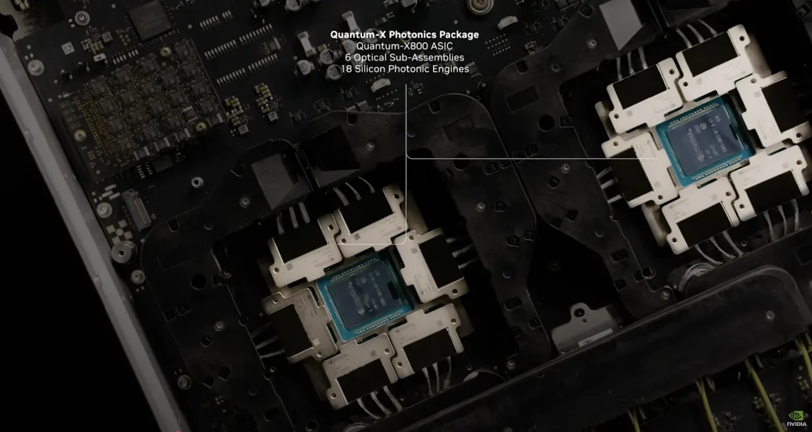
NVIDIA Quantum-X Photonics package and optical subassemblies. The integrated architecture illustrates the relationship between optical and electrical interfaces. Image: NVIDIA, Figure 1.
Learning How to See the Problem Clearly
Before moving into equipment sales, MSSCORPS already had experience building tools for its own analytical workflows. About a decade ago, it developed a laser grooving system to extract samples from packaged chips while better preserving surrounding wiring. It later used low-temperature atomic layer deposition equipment to coat samples with a protective layer, reducing damage caused by preparation before analysis.
These tools address the same underlying requirement: to see the original problem, engineers must first avoid destroying critical evidence during sample extraction and preparation. An electron microscope can be purchased, but getting the structure of interest intact under that microscope still depends on analytical methods and operating experience. MSSCORPS’s customer relationships also developed through this repeated work with samples.
Gino Liu recalls that when a small R&D team at a major foundry customer moved into silicon photonics, MSSCORPS had already worked alongside those engineers on several process projects. Initially, the company even helped with development free of charge, trying to solve the problem first. That gave it an opportunity to encounter difficulties in optical component development early and build the analytical methods customers needed.
Materials analysis typically earns revenue sample by sample. But those services also expose suppliers to requirements that equipment specifications have yet to capture clearly: how a sample should be handled, how a signal should be acquired, and what kind of result would help an engineer decide the next step. As those requirements recur, an internally developed tool can find a path from supporting the laboratory’s work to becoming a product sold outside it.
From Finding a Method to Building a Machine
Zongyu Li, an associate director in MSSCORPS’s silicon photonics engineering division, has described an early obstacle. The team wanted to inject light into a chip but could not successfully couple it into the waveguide using the fiber equipment it had purchased and modified. It made its own lens to reduce the beam size and clear that first hurdle.
The next task was locating where the loss occurred. Li thought of instruments that telecommunications engineers use to locate breaks in optical fibers. He approached an instrument manufacturer, and they spent more than six months adapting the equipment, attempting to bring a measurement method used for long-distance fiber into chip analysis. Even after finding a workable method, much of the engineering remained: the complete machine had to operate reliably.
According to Li, even small movements and shifts in the machine could affect the optical power it collected. The team revised its mechanical design more than ten times to overcome vibration. That illustrates the engineering distance between obtaining a measurement once and building a piece of equipment. If the measurement setup itself is unstable, engineers struggle to distinguish power changes caused by the device under test from those introduced by the test process.
The same issue appears in production testing. Robert Manion, general manager of semiconductor solutions at Emerson’s NI, points to optical coupling and alignment as challenges in silicon photonics testing. Scaling production also requires shortening those steps and increasing automation. MSSCORPS’s R&D diagnostics and the high-volume testing NI addresses have different goals, but both first require light to enter and leave the device under test reliably before subsequent measurements can be useful.
For MSSCORPS, familiarity with customers’ problems tells it what to develop. Integrating optical methods, sample handling, and mechanical stability gives it a tool it can sell. The equipment’s value therefore extends beyond any single precision figure to whether it lets customers repeatedly perform useful analysis.
Bringing the Laboratory to Silicon Valley
MSSCORPS has taken the same approach of staying close to customers into the United States. Its subsidiary MSS USA established a physical laboratory in Sunnyvale, California, and held an opening event in May 2025. Chunhao Liu, MSSCORPS’s chief strategy officer and the CEO of its U.S. company, chose Silicon Valley for a straightforward reason: “Our value lies in R&D. We need to follow the R&D clusters.”
The expansion includes a local team and analytical facilities. Chunhao Liu recruited local staff through LinkedIn and bought a former Siemens laboratory for US$7.3 million. He says the building has six times the electrical capacity of a conventional industrial facility, meeting the needs of its analytical equipment. For a company whose services depend on precision instruments and sample preparation, getting closer to customers requires equipment, people, and operating procedures to be put in place together.
Time creates more immediate pressure. Chunhao Liu says customers ask for results within 24 to 36 hours. If samples still have to be sent back to Taiwan, transport and time differences compress the time available for analysis. Locating a laboratory where customers conduct R&D reduces the wait for international sample shipments and gives results a better chance of arriving in time for the next engineering decision. For designs still undergoing repeated adjustments, when the result reaches the engineer is part of the service’s value.
The division of work between Taiwan and the United States extends to method development. Chunhao Liu says the U.S. team has more room to experiment with new workflows, which can then be transferred to Taiwan once mature. Engineers in the two locations also communicate directly. That gives the U.S. operation the potential to serve customers while developing analytical methods. MSSCORPS is turning some diagnostic capabilities into equipment for sale while bringing its laboratories closer to R&D clusters. The two moves can reinforce each other by keeping the company exposed to new problems and allowing it to build the solutions into its next tools and services.
Selling Some Capabilities While Keeping the Harder Problems
MSSCORPS’s equipment strategy also responds to the revenue characteristics of analytical services. Gino Liu says that handling all analysis in-house requires the company to invest upfront in enough machines. Yet some development-stage demand may decline once a customer’s manufacturing process stabilizes. Selling equipment to customers provides another way to recover development spending.
The company does not intend to transfer every capability at once. Gino Liu describes the division this way: equipment sold externally can handle optical leakage defects at the 100-nanometer scale, while smaller problems below 50 nanometers remain within the company’s laboratory, requiring customers to send samples for analysis. This is the boundary the company draws between equipment and services: customers can handle some needs themselves while more demanding work remains a service.
Whether that arrangement lasts depends on the continued progress of its internal analytical capabilities. Customers who buy equipment gain their own operating experience and may modify the machines themselves. To sustain the value of its services, MSSCORPS needs to keep addressing problems that existing equipment cannot resolve. Equipment sales broaden the use of its technology while raising the demand for its laboratories to keep advancing.
In an earlier interview, Gino Liu specifically explained that this equipment is primarily intended to accelerate R&D and product development. Between growth in the CPO market and orders for MSSCORPS’s machines lie further decisions: how many projects customers launch, who performs the analysis, and whether they want to add equipment of their own. After the initial deliveries, whether customers incorporate the machines into their everyday R&D workflows and continue sending samples when harder problems arise will reveal more about the business’s progress than CPO shipment forecasts alone.
Sources
- Yaoyu Liu, “From Laboratory to Equipment Supplier, Shipping to AI Giants: How MSSCORPS Is Capturing the First Wave of CPO Inspection Business,” Business Weekly, issue 2032, pp. 90–92.
- Bizhu Chen, “From Electrical Leakage to Optical Loss: MSSCORPS’s Six Years Alongside TSMC and Its Close Ties with NVIDIA,” Wealth Magazine, issue 762.
- Elaine I-yun Huang, “MSSCORPS’s 29-Year-Old Second-Generation Leader Gives His Father the Confidence to Establish a U.S. Facility: Taiwan–U.S. Collaboration Delivers 24-Hour Turnaround, While Proprietary Patents Make It an R&D Team’s Choice,” CommonWealth Magazine, issue 850.
- MSSCORPS, “Grand Opening of MSS USA CORP, U.S. Subsidiary of MSSCORPS CO., LTD. – May 7, 2025,” May 7, 2025.
- Micro-Electronics Magazine, “Robert Manion, General Manager of Semiconductor Solutions at Emerson’s Test & Measurement Group: Silicon Photonics Testing Challenges Traditional ATE,” issue 483.
- Ashkan Seyedi, “How Industry Collaboration Fosters NVIDIA Co-Packaged Optics,” NVIDIA, August 26, 2025.